Community
Community
NEWS
총 1014건의 게시물이 있습니다.
There are a total of 1014 posts.
-
Research
Study Reveals Why Perovskite Performance Changes Across Solar Cell Designs 신규게시글Published in Joule, the study traces the performance gap to crystal formation at the underlying interface and demonstrates an inverted cell with 26.3% efficiency.JooHyeon HeoAbstract A perovskite precursor solution that delivers power conversion efficiencies (PCEs) exceeding 26% in conventional nip solar cells exhibits severe performance losses when directly applied to inverted pin architectures, revealing that high-efficiency compositions are not inherently transferable. Here, we identify a buried-interface crystallization mismatch, arising from the distinct physicochemical natures of inorganic SnO2 electron-transporting layers and organic self-assembled hole-transporting monolayers (SA-HTLs), as the origin of this divergence. The methylammonium chloride (MACl)-associated intermediate phase, MA2Pb3I8·2DMSO, persists and decomposes with strong underlayer dependence, stabilizing beneficially on SnO2 but impeding crystallization on SA-HTLs. To overcome this limitation, we develop a chloride-origin engineering strategy that decouples chloride functionality from volatile organic ammonium species by incorporating low-solubility lead chloride (PbCl2) with strong Pb–Cl coordination. This enables controlled interfacial desolvation and nucleation on SA-HTLs, suppresses buried defects, and establishes buried-interface crystallization control as a design principle for architecture-convergent, high-efficiency perovskite solar cells. Building a high-performance solar cell takes more than getting the materials right. The same ingredients can produce very different results when the layers are arranged differently—and researchers at UNIST have discovered why. Led by Distinguished Professor Sang Il Seok of the School of Energy and Chemical Engineering at UNIST, the team found that the surface beneath the light-absorbing perovskite layer can determine how well its crystals form. By tailoring the material chemistry to that surface, the researchers developed an inverted perovskite solar cell with a power conversion efficiency of 26.3% and improved stability. PSCs can be built in conventional nip or inverted pin configurations. Both have reached high efficiencies, but formulations optimized for one do not necessarily perform as well in the other. Inverted cells are particularly important for perovskite–silicon tandem solar cells, where they are commonly used as the top cell. The researchers found that this performance gap originates at the buried interface, where the perovskite layer forms on the material beneath it. A formulation that achieved efficiencies above 26% in conventional cells lost much of its performance when transferred directly to an inverted design. The difference came down in part to methylammonium chloride (MACl), an additive used to improve perovskite crystal growth. In conventional cells, an intermediate formed by MACl supports crystallization on the underlying inorganic layer. But on the organic layer used in inverted cells, the intermediate persists longer, disrupting crystal growth and leaving behind voids and defects that can lead to electrical losses. Rather than removing chloride, the team changed how it was introduced. The researchers reduced the amount of MACl and added a small amount of lead chloride (PbCl2), whose stronger interaction with chloride helped control where and when crystals began to form. This produced a cleaner buried interface with fewer defects. With the revised formulation, the inverted cells reached a peak efficiency of 26.3% and a fill factor of up to 86.8%, while also showing improved stability. The results demonstrate that controlling how perovskite crystals form at the underlying surface can help high-performance materials work across different solar-cell designs. “High-efficiency formulations developed for conventional PSCs do not necessarily behave the same way in inverted devices,” said Professor Seok. “By identifying the origin of this performance loss, we established a way to control crystal formation at the buried interface. The findings provide a design direction for developing efficient inverted cells for high-performance perovskite–silicon tandem solar cells.” Their findings have been published online in Joule on July 28, 2026. The study was supported by the National Research Foundation of Korea (NRF). Journal Reference Jongbeom Kim, Nahye Shin, Chaehoon Jeon, et al ., “Buried-interface crystallization limits the transferability of high-efficiency perovskite precursor compositions,” Joule ,(2026).- 2026.08.19
- 130
-
Research
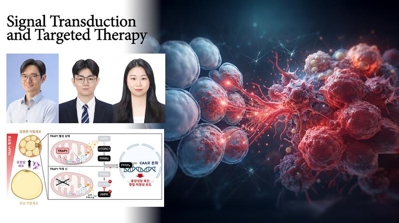
New Study Reveals How Nearby Fat Cells Help Breast Cancer Resist Treatment 신규게시글Published in STTT, the study links TRAP1 inhibition to improved chemotherapy response in breast cancer.JooHyeon HeoAbstract Adipocytes are essential stromal components of the tumor microenvironment (TME) in breast cancer that play pivotal roles in cancer progression and chemoresistance. In close proximity to tumor cells, they undergo phenotypic reprogramming into cancer-associated adipocytes (CAAs), characterized by multilocular lipid droplets, increased mitochondrial content, and elevated expression of uncoupling protein 1 (UCP1). Although these features superficially resemble those of beige adipocytes, they do not recapitulate classical thermogenic programming, reflecting a unique metabolic adaptation driven by the TME. Here, we identified tumor necrosis factor receptor-associated protein 1 (TRAP1), a mitochondrial paralog of HSP90, as a central regulator of the transition of adipocytes into CAAs. TRAP1 was highly upregulated in CAAs and was required to drive a tumor-associated adipocyte secretory program, including the adipokine complement factor D (CFD). Genetic and pharmacological TRAP1 inhibition destabilized the mitochondrial electron transport chain, reduced cellular respiration, and activated the energy sensor AMPK. This subsequently suppressed mTOR and PPARγ signaling, effectively abrogating adipocyte reprogramming and diminishing pro-tumorigenic adipokine secretion. Crucially, this CAA-secreted CFD promoted cancer cell survival and chemoresistance via C3aR-AKT/ERK signaling, and blocking this TRAP1-mediated crosstalk profoundly sensitized breast tumors to chemotherapy in vivo. Collectively, these findings identify TRAP1 as a master regulator of adipocyte transdifferentiation within the TME, offering a novel strategy to restrict tumor growth and overcome drug resistance in breast cancer. Breast tumors can reshape the fat cells around them, creating an environment that helps cancer cells survive and resist chemotherapy. Researchers at UNIST and the National Cancer Center (NCC) have identified a mitochondrial protein that helps drive this transformation—and shown in mice that blocking it can make tumors more responsive to treatment. Led by Professor Byoung Heon Kang of the Department of Biological Sciences at UNIST and Professor Sun-Young Kong of NCC, the team found that TRAP1 plays a key role in converting normal fat cells into cancer-associated adipocytes (CAAs). These altered cell release factors that support tumor growth and protect cancer cells from chemotherapy. The researchers found that TRAP1 sustains mitochondrial energy production in fat cells, keeping the mTOR–PPARγ pathway active and allowing them to acquire cancer-supporting properties. Blocking TRAP1 disrupts mitochondrial function and activates AMPK, an energy sensor that suppresses this transformation. In tissue samples from 31 patients with breast cancer, TRAP1 expression in fat surrounding tumors was 3.03 times higher than in normal adipose tissue. The team also identified complement factor D (CFD) as an important link between the altered fat cells and cancer cells. CAAs secrete CFD, which activates survival signals in breast cancer cells and makes them less susceptible to chemotherapy. Blocking this TRAP1-driven communication reduced that protective effect. In mice, genetically removing TRAP1 suppressed the transformation of adipocytes and reduced tumor weight by as much as 56% compared with controls. Drug-based inhibition produced similar results: combining the TRAP1 inhibitor gamitrinib with cisplatin reduced tumor weight by 76% compared with untreated mice. Another inhibitor, SB-U015, also enhanced the effects of cisplatin and paclitaxel without evident toxicity in the experimental models. “Our study shows how adipocytes surrounding breast tumors can contribute to chemotherapy resistance,” said Professor Kong. “Further studies are needed to evaluate the clinical potential of TRAP1 inhibitors, not only for patients who respond poorly to existing treatments but also for cancers that develop in close contact with adipose tissue, including ovarian, pancreatic, and prostate cancers.” Professor Kang added, “These findings suggest that the cells surrounding a tumor can be important therapeutic targets alongside the cancer cells themselves. By disrupting the metabolic changes in nearby adipocytes, we may be able to improve the effectiveness of existing anticancer drugs.” Professor Kang has transferred the technology arising from the research to SmartinBio, a UNIST faculty startup, where further development of anticancer drug candidates is underway. The study was co-first authored by Dr. Nam Gu Yoon and Dr. So-Yeon Kim of UNIST and published online in Signal Transduction and Targeted Therapy (STTT) on July 28, 2026. The research was supported by the National Research Foundation of Korea (NRF), the National Cancer Center, and the Korea Drug Development Fund (KDDF). Journal Reference Nam Gu Yoon, So-Yeon Kim, So-Youn Jung, et al ., “The pro-tumorigenic functions of cancer-associated adipocytes are dependent on the mitochondrial chaperone tumor necrosis factor receptor-associated protein 1,” STTT., (2026).- 2026.08.18
- 242
-
Research
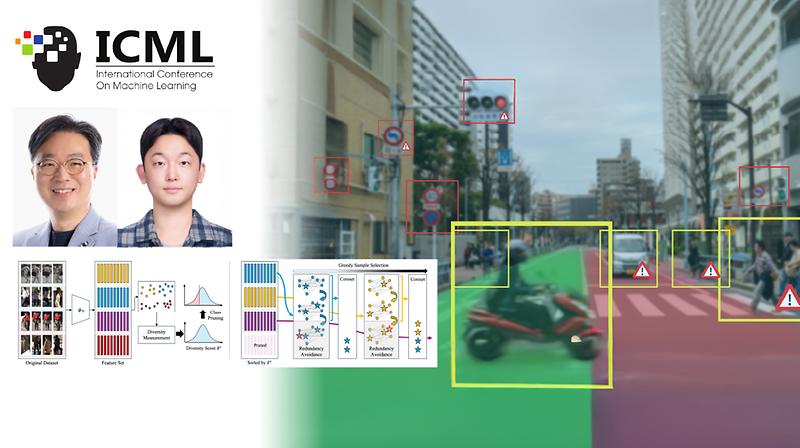
New Framework Reduces Data Needed to Train Re-Identification AI 신규게시글Their findings were accepted for presentation at the ICML '26, which took place in Seoul, from July 6 to 11, 2026.JooHyeon HeoAbstract Coreset Selection (CS) aims to extract a small yet representative subset from a large dataset, reducing the complexity of model training. Although CS has been primarily investigated for classification tasks, it is still underexplored for object Re-identification (ReID). In this paper, we first formulate Coreset Selection for Object Re-identification (CSOR) as a joint optimization problem to find both the optimal coreset and the optimal class subset. We identify intra-class diversity as a key factor for effective coreset construction for ReID. Based on this insight, we propose a novel two-stage framework, consisting of Diversity-driven Class Pruning (DCP) and Coverage-Prioritized Sampling (CPS), to address the unique challenges of ReID datasets. First, classes with low feature diversity are pruned to allocate the storage budget to the remaining informative classes. Then, samples are greedily selected in an easy-to-hard class order to maximize feature coverage within each class. Extensive experiments on three person ReID datasets and one vehicle ReID dataset demonstrate that our method consistently outperforms existing CS approaches, establishing a new state-of-the-art in CSOR. Video datasets used to train re-identification systems often contain near-duplicate images. The same person or vehicle may appear across many consecutive frames with little change, increasing storage and computing demands without adding equally useful information. Led by Professor Jae-Young Sim in the UNIST Graduate School of Artificial Intelligence, the research team has developed a method that filters out much of this redundancy, while preserving the visual diversity needed for training. The method, called Coreset Selection for Object Re-identification (CSOR), selects a compact set of representative images from a much larger dataset. Object re-identification (ReID) enables AI systems to match the same person or vehicle across different camera views. Unlike image classification, ReID models must distinguish identities they have never encountered during training. This makes conventional coreset methods—which were developed largely for classification—difficult to apply directly. “Re-identification models must distinguish entirely new people or vehicles that were not included in the training data,” said first author Minyoung Oh, a researcher at UNIST. “We began with this distinction and redesigned the selection criteria around the specific demands of ReID.” The researchers formulated CSOR as a joint optimization problem that determines both which identity classes and which images to retain. Their analysis identified diversity within each class—the range of appearances captured for the same person or vehicle—as a key factor in building an effective training subset. CSOR follows a two-stage process. Diversity-driven Class Pruning (DCP) first removes identity classes with little feature variation, preserving more of the storage budget for classes with richer information. Coverage-Prioritized Sampling (CPS) then selects images from the remaining classes, giving priority to those that capture the broader range of features. The team evaluated CSOR on three person and one vehicle ReID datasets. The method consistently outperformed the CS approaches used for comparison. Models trained on approximately half of the original data retained more than 95% of the performance achieved using the full dataset. “ReID datasets are commonly built from video, so duplicate images accumulate quickly as the same person or vehicle appears across consecutive frames,” said Professor Sim. “CSOR removes much of this repetition while retaining the diversity needed for ReID. It could make training and deployment more practical on edge devices with limited storage and computing resources.” Their findings were accepted for presentation at the 2026 International Conference on Machine Learning (ICML), held at COEX in Seoul in July 2026. The study was supported by the National Research Foundation of Korea (NRF) and the Institute for Information & Communications Technology Planning & Evaluation (IITP), with funding from the Ministry of Science and ICT (MSIT). Support was provided through the Mid-Career Researcher Program, the AI Graduate School Program, the AI Star Fellowship Program, and an initiative for training in industrially integrated multimodal generative AI. Journal Reference Minyoung Oh and Jae-Young Sim, "CSOR: Coreset Selection for Object Re-identification via Class Pruning," ICML '26 , (2026).- 2026.08.14
- 784
-
Research
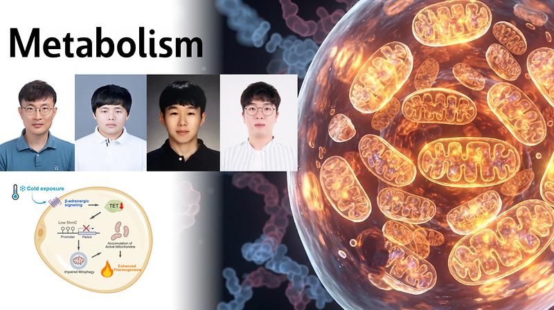
Cold-Sensitive Epigenetic Pathway Regulates Heat Production in Fat 신규게시글Their findings have been published online in Metabolism on July 1, 2026.JooHyeon HeoAbstract Adipose tissue thermogenesis is a major determinant of energy homeostasis, and its dysregulation contributes to obesity and metabolic disease. Parkin-mediated mitophagy is required for thermogenic adaptation, but the upstream mechanisms linking thermal cues to this pathway remain poorly defined. Here, we identify the ten-eleven translocation (TET) family of DNA dioxygenases as thermosensitive epigenetic regulators of Prkn transcription in adipocytes. Cold exposure coordinately suppressed TET expression and reduced global 5-hydroxymethylcytosine (5hmC) levels in white and brown adipose tissue through β-adrenergic signaling. Adipose-specific TET triple-knockout mice exhibited enhanced white fat begging, brown fat activation, increased energy expenditure, and improved cold tolerance. Transcriptomic network analysis identified Parkin as a key mitophagy node in TET-deficient adipose tissue. Consistent with this, loss of adipose TET reduced Parkin expression, impaired mitophagic flux, and promoted accumulation of metabolically active mitochondria with increased respiratory capacity. Mechanistically, TET proteins occupied the Prkn promoter and maintained a transcriptionally permissive state through catalytic conversion of 5-methylcytosine to 5hmC, whereas TET loss increased promoter methylation and suppressed Prkn expression. Re-expression of wild-type, but not catalytically inactive, Parkin largely normalized mitochondrial content and respiratory activity in TET-deficient adipocytes. Together, these findings define a thermosensitive TET-Parkin epigenetic axis that links environmental cold signals to mitochondrial quality control during adaptive thermogenesis. Cold exposure prompts fat cells to burn more energy and generate heat. Researchers at UNIST have identified a molecular pathway that helps these cells retain more mitochondria, sustaining their heat-producing capacity. Led by Professor Myunggon Ko of the Department of Biological Sciences at UNIST, the team found that TET proteins, a family of enzymes that regulate DNA modifications, control the expression of Parkin, a key protein involved in mitochondrial removal. When cold reduces TET levels in fat cells, Parkin levels also fall, allowing more metabolically active mitochondria to remain. Published in the July 2026 issue of Metabolism , their findings reveal a previously unknown link between environmental temperature and mitochondrial quality control in adipose tissue. White fat primarily stores excess energy, while brown fat burns energy to produce heat. Under cold conditions, some white fat cells can acquire heat-producing properties, becoming beige fat. This transition is accompanied by an increase in mitochondria, which supply the energy needed for heat production. The researchers found that cold suppresses TET expression in both white and brown adipose tissue through β-adrenergic signaling. Levels of 5-hydroxymethylcytosine (5hmC)—a DNA modification associated with TET activity—also decline. TET proteins normally act at the Prkn gene promoter, where they help maintain Parkin expression by converting 5-methylcytosine to 5hmC. When TET levels fall, methylation increases at the promoter and Parkin expression declines. Parkin plays a central role in mitophagy, the process cells use to selectively remove mitochondria. With less Parkin available, mitophagy slows, allowing more mitochondria to accumulate in fat cells. The effect was evident in mice lacking all three TET proteins specifically in adipose tissue. Compared with control mice, they showed increased becoming of white fat, greater brown-fat activation, higher energy expenditure, and better tolerance to cold. Their adipose tissue also contained less Parkin, along with increased mitochondrial DNA and proteins involved in cellular respiration. Cell-based experiments further confirmed Parkin's role in the pathway. Restoring functional Parkin in TET-deficient adipocytes largely returned mitochondrial abundance and oxygen consumption to normal levels, while a catalytically inactive form of Parkin did not. This showed that Parkin is a key link between TET activity and mitochondrial turnover. “Cold-induced increases in mitochondria and thermogenesis in adipose tissue have been well documented, but the upstream mechanism controlling these changes has remained unclear,” said Professor Ko. “Our findings identify TET proteins as part of that regulatory system and reveal how changes in Parkin-mediated mitochondrial turnover contribute to the thermogenic response.” Professor Ko added that understanding this pathway could inform future research into metabolic diseases such as obesity and type 2 diabetes, where increasing energy expenditure in adipose tissue has been explored as a potential therapeutic strategy. The study was supported by the Ministry of Science and ICT (MSIT) and the National Research Foundation of Korea (NRF), among other funding sources. Journal Reference Seongjun Byun, Chan Hyeong Lee, Kyumin Jang, et al., “A thermosensitive TET–Parkin epigenetic axis couples mitochondrial quality control to adaptive thermogenesis in adipose tissue,” Metabolism, (2026).- 2026.08.12
- 1179
-
Research
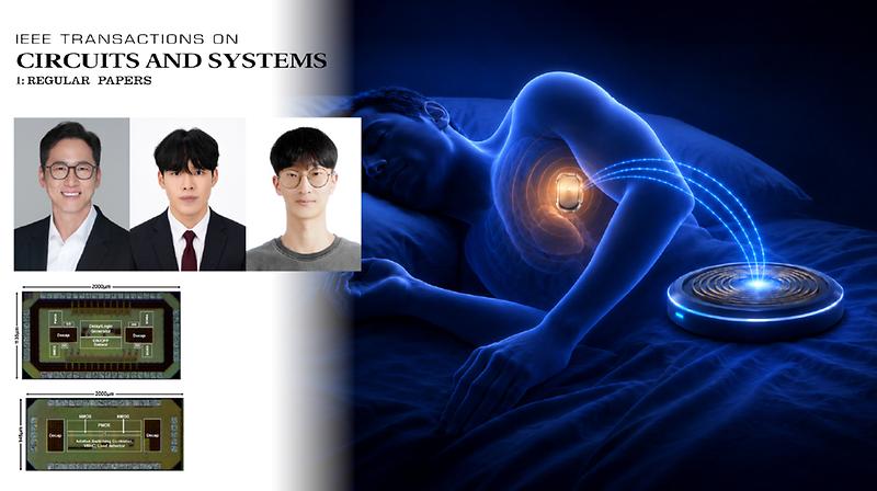
Adaptive Wireless Charging for Implantable Medical Devices 신규게시글Their findings were published in IEEE TCAS-I on June 19, 2026.JooHyeon HeoAbstract This paper presents a wireless power transfer (WPT) system that maintains high efficiency and low output voltage ripple under large variations in coupling and load conditions. To address these variations, the proposed system employs an adaptive mode switching scheme with coupling-insensitive sensing. This is implemented using a fixed-reference sensor topology with filtered integrated sensor outputs and synchronization of RX 0X-to-1X transitions with TX 0X-to-1X mode transitions. For stable output regulation, a voltage-racing hysteretic controller is introduced to achieve low output voltage ripple, which is difficult to obtain with conventional analog feedback- or comparator-based hysteretic controllers. In addition, an on-chip load detector enables automatic detection of heavy- and light-load conditions. Fabricated in a 0.18- μ m BCD process, the proposed system was measured with coil distances from 7 to 20 mm, corresponding to coupling coefficient (k) variations from 0.42 to 0.08. The system supports an output power range from 2.6 mW to 147 mW while achieving a low ripple voltage of 18 mV and achieves a peak end-to-end efficiency of 69.1%. Implantable medical devices must continue operating reliably despite the body's constant movement—from walking and breathing to simply changing position during sleep. But those everyday movements can disrupt wireless charging by altering the alignment between the external charger and the implanted device. Researchers at UNIST have developed a wireless power transfer system that adapts to changes in body movement and device power demand. By maintaining stable power delivery while reducing unnecessary energy loss and heat generation, the system could make long-term wireless powering of implantable medical devices more practical. Many implantable medical devices alternate between active treatment and standby modes, causing their power requirements to change over time. At the same time, body movement can shift the distance or alignment between the transmitter and receiver coils, reducing wireless charging efficiency. Together, these challenges make it difficult to deliver stable power when and where it is needed. Led by Professor Franklin Bien of the Department of Electrical Engineering, the team designed the system to distinguish changes in device power demand from changes in coil alignment caused by body movement. Rather than relying solely on signal strength, it detects characteristic changes in communication between the transmitter and receiver, allowing it to switch reliably between high- and low-power modes as charging conditions change. The researchers also developed a new Voltage-Racing Hysteretic Controller (VRHC) to stabilize the receiver's output voltage. Instead of comparing voltages directly, the new controller detects voltage changes by measuring tiny differences in signal propagation time within the circuit. This allows it to respond more quickly and keep the output voltage remarkably stable. In laboratory tests, the system remained stable across transmission distances ranging from 7 mm to 20 mm. Even when the implanted device's operating current increased sharply from 6 mA to 16 mA, it maintained a constant 3.3 V output with a voltage ripple of only 18 mV. The system achieved a peak end-to-end power transfer efficiency of 69.1%, representing an improvement of up to 51.3 percentage points over a comparable design without the adaptive mode-switching technology. “Wireless charging systems need to adapt as conditions change, whether because a patient moves or a device's power demand shifts,” said Professor Bien. "By continuously adjusting power delivery in real time, our system improves both efficiency and stability. We hope it will help make implantable medical devices more practical for long-term use." The study was co-first authored by Sungmin Shin and Seongbin Kwon of UNIST. The research was supported by the Ministry of Science and ICT (MSIT) and the Institute for Information & Communications Technology Planning & Evaluation (IITP), and published in IEEE Transactions on Circuits and Systems I: Regular Papers (IEEE TCAS-I) on June 19, 2026. Journal Reference Sungmin Shin, Seongbin Kwon, Kiju Lee, et al ., "A Wireless Power Transfer System With Adaptive Mode-Switching Insensitive to Coupling Variations Achieving Low Ripple and High Efficiency," IEEE TCAS-I, (2026).- 2026.08.11
- 1051
-
Research
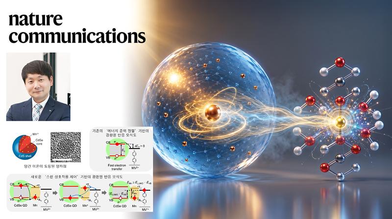
A New Way to Harness Hot ElectronsPublished in Nat. Commun., the findings reveal a new pathway for using short-lived hot-electron energy in light-driven chemical reactions.JooHyeon HeoAbstract Spin-active dopants offer a powerful yet largely unexplored route for controlling interfacial redox chemistry in quantum-confined semiconductors. Here we show that manganese doping in cadmium selenide quantum dots enables an ultrafast spin-exchange-mediated electron-transfer pathway that allows methyl viologen reduction even when conventional band-edge energetics are unfavorable for charge transfer. Femtosecond transient absorption spectroscopy reveals that manganese dopants accelerate electron-transfer dynamics by more than an order of magnitude while opening a hot-exciton reduction channel in which a manganese ion captures a photoexcited exciton prior to phonon-assisted cooling. Subsequent spin-flip relaxation of the excited manganese ion drives charge separation and reduction of a molecular acceptor. This mechanism operates efficiently across resonant and off-resonant (energy-uphill and downhill) regimes, identifying spin-exchange coupling—rather than band alignment—as the dominant factor governing electron-transfer rates and efficiencies. These findings establish magnetic doping as a viable strategy for harvesting hot carriers and enabling energetically demanding photocatalytic transformations. For decades, researchers have understood electron transfer in photocalysis through one guiding principle. Electrons move most readily when the energy levels of a semiconductor and a reacting molecule are well matched. Researchers at UNIST and Los Alamos National Laboratory (LANL) have demonstrated that spin interactions can provide an alternative pathway, allowing electron transfer even when conventional energy-level alignment is unfavorable. Professor Ho Jin of the Department of Chemistry at UNIST, in collaboration with Dr. Victor I. Klimov of LANL, showed that manganese ions inside semiconductor quantum dots (QDs) create an ultrafast spin-exchange pathway that channels hot-electron energy into photoreduction reactions. The findings offer a new way to design photocatalysts that make better use of sunlight for hydrogen production and carbon dioxide conversion. QDs readily transfer photoexcited electrons to nearby molecules, making them attractive materials for photocatalysis. Their most energetic electrons, however, lose excess energy almost immediately, leaving little time for useful chemical reactions to occur. The team addressed this challenge by introducing magnetic manganese ions into cadmium selenide (CdSe) QDs. Before hot electrons could cool, the manganese ions captured their excess energy through ultrafast spin exchange. As the ions returned to their original spin state, that energy drove electrons into nearby molecules, triggering photoreduction reactions that would otherwise be difficult to achieve. Using femtosecond transient absorption spectroscopy, the researchers followed the electron transfer process in real time. Compared with undoped QDs, manganese-doped particles transferred electrons to methyl viologen more than ten times faster, demonstrating that spin exchange provides an efficient pathway for charge transfer. The team then asked whether the mechanism truly depended on hot-electron energy. When larger QDs were illuminated with higher-energy light, photoreduction readily occurred. Under lower-energy illumination, the reaction largely disappeared. Together, these experiments showed that manganese captures the excess energy of hot electrons before it is lost as heat. “We have traditionally thought of energy-level alignment as the deciding factor in electron transfer,” said Professor Jin. “Our results show that spin exchange can provide an alternative pathway, giving us a new way to harness the energy of hot electrons for photocatalysis.” Professor Ho Jin served as the first author of the study. Their findings were published in Nature Communications on June 26, 2026. Journal Reference Ho Jin, Valerio Pinchetti, Connor Orrison, et al., “Ultrafast photoreduction driven by interfacial spin exchange in manganese-doped quantum dots,” Nat. Commun., (2026).- 2026.08.10
- 1415
-
Research
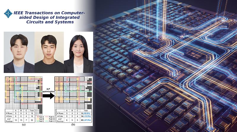
Smarter Design Method Improves Efficiency of In-Memory Computing ChipsThe findings were published online in IEEE TCAD on June 2, 2026.JooHyeon HeoAbstract Data-centric applications continue to be limited by the memory wall. Logic-in-Memory (LiM) architectures based on non-volatile memories (NVMs), such as memristors, offer a promising solution by enabling in-memory computation and eliminating costly data movement. While several approaches leveraging memristor-aided logic (MAGIC) operations have been proposed, many fail to fully exploit the parallelism and spatial efficiency of memristor crossbars, especially under physical design constraints. In this paper, we propose a parallelism-driven, area-aware look-up table (LUT)-based mapping framework of arbitrary logic circuits into a memristor crossbar using MAGIC operations. We present a crossbar-aware floorplanning strategy that leverages topological LUT information to enable two-directional parallel computation (ie, HNOR and VNOR), thereby maximizing computational LUTs with minimal execution cycles. We formulate an integer linear programming (ILP) approach to define the placement of each LUT and its fanin locations, improving routability while preserving parallelism. Moreover, we introduce our novel A∗-search-based fan-in routing method with Hanan grid that fully utilizes the aligned fans and intermediate results. Experimental results demonstrate that the proposed framework achieves maximum parallelism and crossbar utilization, thereby reducing cycle counts by 19.6% and ensuring that all benchmarks map successfully under strict area constraints. We also confirm the scalability and practical applicability of the proposed framework for large-scale logic mapping in memristor-based LiM systems. Modern computing is increasingly limited not by processing speed, but by the time and energy required to move data between memory and processors. Researchers at UNIST have developed an automated design framework that addresses this challenge by making logic-in-memory (LiM) chips more efficient. Led by Professor Heechun Park of the Department of Electrical Engineering, the team designed a framework that automatically optimizes the placement of logic circuits and data pathways in memristor-based LiM architectures. By enabling more operations to run simultaneously while making better use of limited chip area, the approach reduced the number of computation cycles by nearly 20% compared with existing state-of-the-art methods. Unlike conventional computer chips, LiM architectures perform computation directly where data are stored, reducing costly data movement between memory and processors. This approach helps overcome the memory wall where data transfer limits overall computing performance. The framework determines where computations are performed within a memristor crossbar array and how intermediate results move to the next operation. Unlike previous approaches, it enables computations to proceed in both the horizontal and vertical directions, allowing more operations to run simultaneously while making better use of the available chip area. The framework also reorganizes intermediate data during computation, freeing unused memory cells and reducing wasted space. It then identifies efficient routes for transferring intermediate results between computational blocks, preserving parallel execution even under tight area constraints. In benchmark evaluations, chips designed using the new framework required 19.6% fewer computation cycles than those designed using existing approaches. The framework also successfully mapped every benchmark circuit, including designs that previous methods could not accommodate under the same area constraints, suggesting it can scale to larger LiM systems. “The performance of LiM computing depends not only on the memory device itself, but also on how computations are organized within the array,” said Professor Park. "By arranging operations to maximize parallel execution, our framework improves efficiency while remaning practical under realistic area constraints." The research was conducted by Ikkyum Kim and Minhong Kim as first and second authors, respectively, with Professor Heechun Park serving as the corresponding author. The findings were published online in IEEE Transactions on Computer-Aided Design of Integrated Circuits and Systems (IEEE TCAD) on June 2, 2026. The research was supported by the National Research Foundation of Korea (NRF) and the Institute of Information & Communications Technology Planning & Evaluation (IITP). The EDA tool was supported by the IC Design Education Center (IDEC). Journal Reference Ikkyum Kim, Minhong Kim, and Heechun Park, “A Parallelism-Driven, Area-Aware Technology Mapping Framework for Memristive Logic-in-Memory,” IEEE TCAD , (2026).- 2026.08.06
- 2890
-
Research
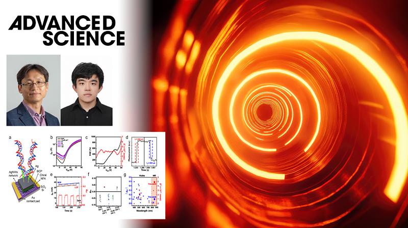
New Organic Photodetector Improves Polarized Near-Infrared Light DetectionTheir findings have been published online in Advanced Science on June 28, 2026.JooHyeon HeoAbstract Near-infrared (NIR) circularly polarized light (CPL) photodetection is of great importance due to its broad application potential in bioimaging, wearable healthcare, optical communication, and advanced optoelectronic systems. In this study, a supramolecular chirality evolution strategy in chiral low-bandgap fused-ring conjugated molecules (LFCs) is presented for high-performance NIR CPL photodetection using Schottky barrier vertical organic field-effect transistors (SB-VOFETs). Halogen substitution combined with thermal annealing drives inversion and amplification of supramolecular chirality in enantiopure LFC thin films. F-substituted LFCs exhibit progressive domain growth and hierarchical ordering with increasing annealing temperature, whereas Cl-substituted LFCs show limited structural evolution above 150°C. These distinct crystallization behaviors directly correlate with chiroptical responses, with F-substituted LFCs achieving a maximum absorption dissymmetry factor (|gabs|) of ∼0.1. When integrated into SB-VOFETs, the optimized chiral films enable highly efficient NIR CPL photodetection, delivering a photocurrent dissymmetry factor (|gph|) of ∼0.1, a specific detectivity of 4.9 × 10¹¹ Jones, an external quantum efficiency exceeding 900%, and a fast response time of ∼600 µs at 850 nm. These metrics represent the highest performance reported for NIR CPL. This study provides design guidelines for advancing high-performance chiral optoelectronic devices through the synergistic integration of atomic substitution, thermal annealing, and device architecture engineering. Near-infrared (NIR) circularly polarized light (CPL) carries information that conventional light cannot, making it valuable for applications ranging from autonomous vehicle sensors and bioimaging to optical security and advanced communications. Detecting this light accurately, however, has remained difficult because the organic semiconductor films used in these devices often lose the molecular order needed to distinguish different polarization states. A research team, led by Professor BongSoo Kim of the Department of Chemistry at UNIST and Professor Joon Hak Oh of Seoul National University has found a way to overcome that limitation. By controlling how chiral organic semiconductor molecules organize within thin films, the researchers significantly improved the films' ability to distinguish between left- and right-handed CPL. When incorporated into a photodetector, the optimized films delivered what the team reports as the highest performance yet achieved for NIR CPL detection. Unlike conventional light detectors, CPL can distinguish between two different polarization states of light. This additional information can reveal not only an object's shape but also properties, such as its surface composition or molecular structure, making the technology valuable for sensing and imaging applications. The researchers achieved the improvement by applying a simple thermal annealing process to thin films made from fluorine-substituted chiral organic semiconductor molecules. Rather than remaining randomly arranged, the molecules reorganized into larger, more ordered crystal domains. This more ordered molecular arrangement strengthened the film's interaction with CPL. As a result, the film's ability to selectively absorb CPL increased more than threefold after annealing at 250°C, with its absorption dissymmetry factor rising from approximately 0.03 to 0.1. Structural analysis confirmed that the annealed films adopted a highly ordered molecular arrangement closely resembling that of single crystals. The researchers also discovered an unexpected effect. As the molecular packing reorganized, the film reversed the polarization it preferentially absorbed, demonstrating that heat treatment could control not only the strength but also the handedness of the material's optical response. By comparison, similar films containing chlorine instead of fluorine showed little structural change above 150°C and exhibited lower polarization selectivity after annealing. To turn these improved optical properties into measurable electrical signals, the team integrated the optimized films into a vertical organic transistor. The device architecture efficiently collected and amplified charges generated by incoming light, allowing the detector to fully capitalize on the improved molecular organization. The resulting photodetector achieved a photocurrent dissymmetry factor of 0.1 at a wavelength of 850 nanometers, demonstrating excellent discrimination between left- and right-handed CPL. It also recorded a specific detectivity of 4.9 × 10¹¹ Jones, an external quantum efficiency of up to 909%, and a response time of less than 600 microseconds—the highest performance reported to date for NIR CPL detectors. “We found that simply controlling how the molecules organize within a thin film can dramatically improve how the materials respond to CPL,” the research team said. “We hope this strategy will help advance next-generation optical sensors and imaging technologies that rely on precise light detection.” Their findings were published online in Advanced Science on June 28, 2026. The research was supported by the National Research Foundation of Korea (NRF) and the Ministry of Science and ICT (MSIT). Journal Reference Jaeyong Ahn, Kwangmin Kim, Sangwook Lee, et al ., “Thermally Driven Supramolecular Chirality Evolution in Low-Bandgap Fused-Ring Conjugated Molecules for High-Performance NIR Circularly Polarized Light Detection,” Adv. Sci., (2026).- 2026.08.05
- 3859
-
Research
New Benchmark Reveals Limits in How AI Understands HandsAccepted to CVPR 2026, HandVQA uses more than 1.6 million questions to expose gaps in spatial reasoning and improve AI performance on previously unseen hand-related tasks.JooHyeon HeoAbstract Understanding the fine-grained articulation of human hands is critical in high-stakes settings such as robot-assisted surgery, chip manufacturing, and AR/VR-based human-AI interaction. Despite achieving near-human performance on general vision-language benchmarks, current vision-language models (VLMs) struggle with fine-grained spatial reasoning, especially in interpreting complex and articulated hand poses. We introduce HandVQA, a large-scale diagnostic benchmark designed to evaluate VLMs' understanding of detailed hand anatomy through visual question answering. Built upon high-quality 3D hand datasets (FreiHAND, InterHand2.6M, FPHA), our benchmark includes over 1.6M controlled multiple-choice questions that probe spatial relationships between hand joints, such as angles, distances, and relative positions. We evaluate several state-of-the-art VLMs (LLaVA, DeepSeek and Qwen-VL) in both base and fine-tuned settings, using lightweight fine-tuning via LoRA. Our findings reveal systematic limitations in current models, including hallucinated finger parts, incorrect geometric interpretations, and poor generalization. HandVQA not only exposes these critical reasoning gaps but provides a validated path to improvement. We demonstrate that the 3D-grounded spatial knowledge learned from our benchmark transfers in a zero-shot setting, significantly improving accuracy of model on novel downstream tasks like hand gesture recognition (+10.33%) and hand-object interaction (+2.63%). Understanding a human hand gesture requires more than recognizing fingers. An AI model must also make sense of how those fingers bend, how joints related to one another, and how the entire hand changes with viewpoint. Current vision-language models remain surprisingly weak at this kind of finger-grained reasoning. A research team, led by Professor Seungryul Baek of the Graduate School of Artificial Intelligence at UNIST has developed HandVQA, a new benchmark that tests this ability in detail. Drawing on 3D hand data, the benchmark contains more than 1.6 million questions about joint angles, distances, and relative positions. It also gives researchers a way to improve the skills it is designed to measure. Despite strong performance on general image-and-language tasks, vision-language models can struggle when spatial differences become subtle. Existing benchmarks rarely examine hand anatomy at the level of individual joints, making these weaknesses difficult to measure. HandVQA fills that gap with questions generated from hand images and precise 3D joint coordinates. For each image, the benchmark asks 25 questions about properties such as finger flexion, the distance between joints, and whether one joint is above, below, in front of, or behind another. The results showed just how much current models miss. Without specialized training, several leading vision-language models performed near chance on some spatial questions and had particular difficulty judging distances between joints. They also made geometric errors and, in some cases, referred to finger parts that did not exist in the image. But the same benchmark that exposed these weaknesses also helped correct them. After LLaVA was fine-tuned with HandVQA, its accuracy on questions about joint distances increased from 16.20% to 90.79%. The benefits also carried over to tasks outside the benchmark. Qwen-VL, after learning from HandVQA, improved on two tasks it had not been directly trained for: hand gesture recognition by 10.33 percentage points and hand-object interaction by 2.63 percentage points. This transfer suggests that the model learned a broader understanding of hand geometry rather than simply becoming better at answering HandVQA questions. “HandVQA not only helped the model answer questions it had previously struggled with, but also improved its ability to handle new tasks,” said MD Khalequzzaman Chowdhury Sayem, first author of the study. “The spatial knowledge learned from the benchmark transferred to other hand-related tasks without requiring additional task-specific training.” Professor Baek added, “Accurately understanding hand pose is important in applications where even small errors can matter, from robotic manipulation and AR/VR interfaces to assistive technologies. HandVQA helps identify where current models fall short and provides a way to improve those capabilities.” Their findings have been accepted to the IEEE/CVF Conference on Computer Vision and Pattern Recognition (CVPR) 2026, one of the leading international conferences in computer vision. The study was supported by the National Research Foundation of Korea (NRF) through the Mid-Career Researcher Program and the Basic Science Research Program, along with programs administered by the Institute for Information communication Technology Planning and Evaluation (IITP), including the AI Star Fellowship, AI Graduate School, and the LG AI STAR Talent Development Program for Leading Large-Scale Generative AI Models in the Physical AI Domain programs. Journal Reference MD Khalequzzaman Chowdhury Sayem, Mubarrat Tajoar Chowdhury, et al. , “HandVQA: Diagnosing and Improving Fine-Grained Spatial Reasoning about Hands in Vision-Language Models,” CVPR '26, (2026).- 2026.08.04
- 5110
-
Research
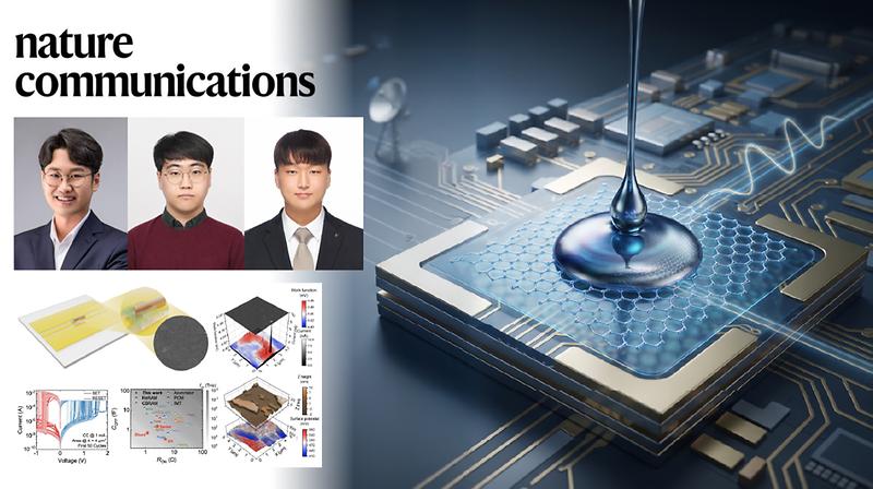
Solution-Processed Semiconductor Enables High-Performance RF Switches for 6G and Satellite CommunicationsTheir findings have been published online in Nature Communications on June 18, 2026.JooHyeon HeoAbstract Next-generation 6G communication requires radio-frequency components capable of operating above 100 GHz with low loss, high isolation, and zero static power—requirements that challenge complementary metal-oxide-semiconductor (CMOS) and microelectromechanical systems (MEMS) technologies. Here, we report transfer-free, large-area millimeter-wave (mmWave) switches based on solution-processed MoS2. While solution-processed 2D materials are often viewed as inferior to their crystalline counterparts due to high defect densities, we demonstrate that their edge-rich morphology is, in fact, a performance enabler. These edge defects act as intrinsic templates that confine Cu-filament pathways, enabling rapid (76 ns) and low-energy switching (1.57 nJ) with > 2000 cycles and uniform zero static-power operation, as corroborated by Kelvin probe force microscopy, conductive atomic force microscopy and low-temperature studies. The resulting switches achieve an low insertion loss ( < 0.1 dB) and high isolation ( > 35 dB) at 67 GHz. Notably, they exhibit a switching figure-of-merit (RON·COFF) of ~ 0.8 fs (fco ~ 187 THz), surpassing previously reported 2D switches. Importantly, by adopting an inverse-state operational scheme in a SHUNT architecture, we mitigate self-switching and achieve improved power handling (P0.1dB > 10 dBm) and linearity (IIP3 > 42.1 dBm). Finally, we demonstrate the platform's circuit-level viability by integrating the switches into a true-time-delay and hybrid-coupled phase shifters targeting 30 GHz mmWave applications. Researchers at UNIST have developed a high-performance radio-frequency (RF) switch using a solution-processed two-dimensional (2D) semiconductor, demonstrating stable operation at frequencies up to 67 GHz while consuming no static power. The technology could support future 6G wireless networks, satellite communications, radar systems, and other high-frequency communication platforms that demand compact, energy-efficient components. Led by Professor Myungsoo Kim of the Department of Electrical Engineering, the team fabricated the device using a thin film of solution-processed molybdenum disulfide (MoS2). Unlike conventional fabrication methods that require 2D semiconductor films to be grown and transferred onto a substrate, the new approach forms the semiconductor layer directly from a liquid precursor, simplifying manufacturing and making large-area production more practical. RF switches are fundamental components in wireless communication systems. They control the flow of high-frequency signals in smartphones, wireless base stations, satellite communications, radar systems, and autonomous vehicles. As communication technologies move toward the millimeter-wave frequencies required for future 6G and space communications, RF switches must transmit signals with minimal loss, effectively block unwanted leakage, and operate with very low power consumption. The newly developed switch achieved all three. Operating at 67 GHz, it recorded an insertion loss below 0.1 dB and signal isolation greater than 35 dB, allowing nearly all of the incoming signal to pass while suppressing signal leakage to less than 0.03%. The device also requires no standby power. Once switched on or off, it maintains its operating state even after power is removed, reducing unnecessary energy consumption. The researchers attribute the device's durability to the characteristics of the solution-processed MoS2 film. During fabrication, naturally occurring sulfur vacuums help guide the movement of copper ions that create the conductive pathways responsible for switching. Rather than reducing performance, these defects stabilize the switching process. Devices fabricated using solution-processed films continued to operate reliably after more than 2,000 switching cycles, whereas comparable devices fabricated from mechanically exfoliated MoS2 showed a lifetime of only about 100 cycles. To evaluate its practical potential, the team integrated the switch into communication circuits used for high-frequency signal control, including a transmit/receive switch and a beam-steering phase shifter. Both operated successfully, demonstrating that the technology can be incorporated into circuits used in satellite communications, radar, defense systems, and future wireless networks. Beam-steering phase shifters electronically direct radio waves without physically moving the antenna, enabling fast and precise tracking of moving targets such as satellites and drones. “By using solution-processed 2D semiconductor materials, we developed an RF switch that combines low signal loss with excellent isolation in the millimeter-wave band without requiring complex transfer processes,” said Professor Kim. “Because the switch retains its operating state even when power is removed, it consumes no standby power and could contribute to smaller, more energy-efficient communication systems for 6G, satellite communications, radar, and defense applications.” The findings were published online in Nature Communications on June 18, 2026. The research was supported by the National Research Foundation of Korea (NRF) and the Institute of Information & Communications Technology Planning & Evaluation (IITP), including the Space-K BIG Project and the InnoCORE Program of the Ministry of Science and ICT (MSIT). Journal Reference Changwoo Pyo, Sungmoon Park, Seungchan Lee, et al ., "Sub-femtosecond figure-of-merit millimeter-wave switches via solution-processed MoS2 for 6G radio-frequency front-ends," Nat. Commun ., (2026).- 2026.08.03
- 4923